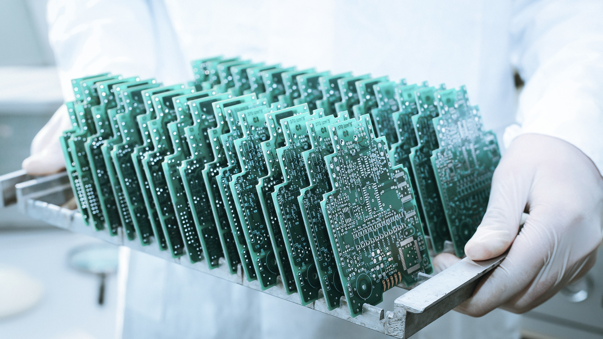
PCB Etching
Deep Dive into PCB Manufacturing in the Semiconductor Industry
JHY adheres to a philosophy of social responsibility and sustainable development. We actively collaborate with upstream and downstream customers, universities, and research institutes. As the holder of several patents and one of the drafting units of national standards, we have developed several technologies and possess a team of professional technical service consultants. We provide one-on-one customized technical support solutions and joint development to assist semiconductor production lines achieve technological breakthroughs.
|
The Secret Weapon of Tech Giants
Discover the Following Solution
|
 |
The Exceptional Performance of JHY's electronic-grade Potassium Monopersulfate
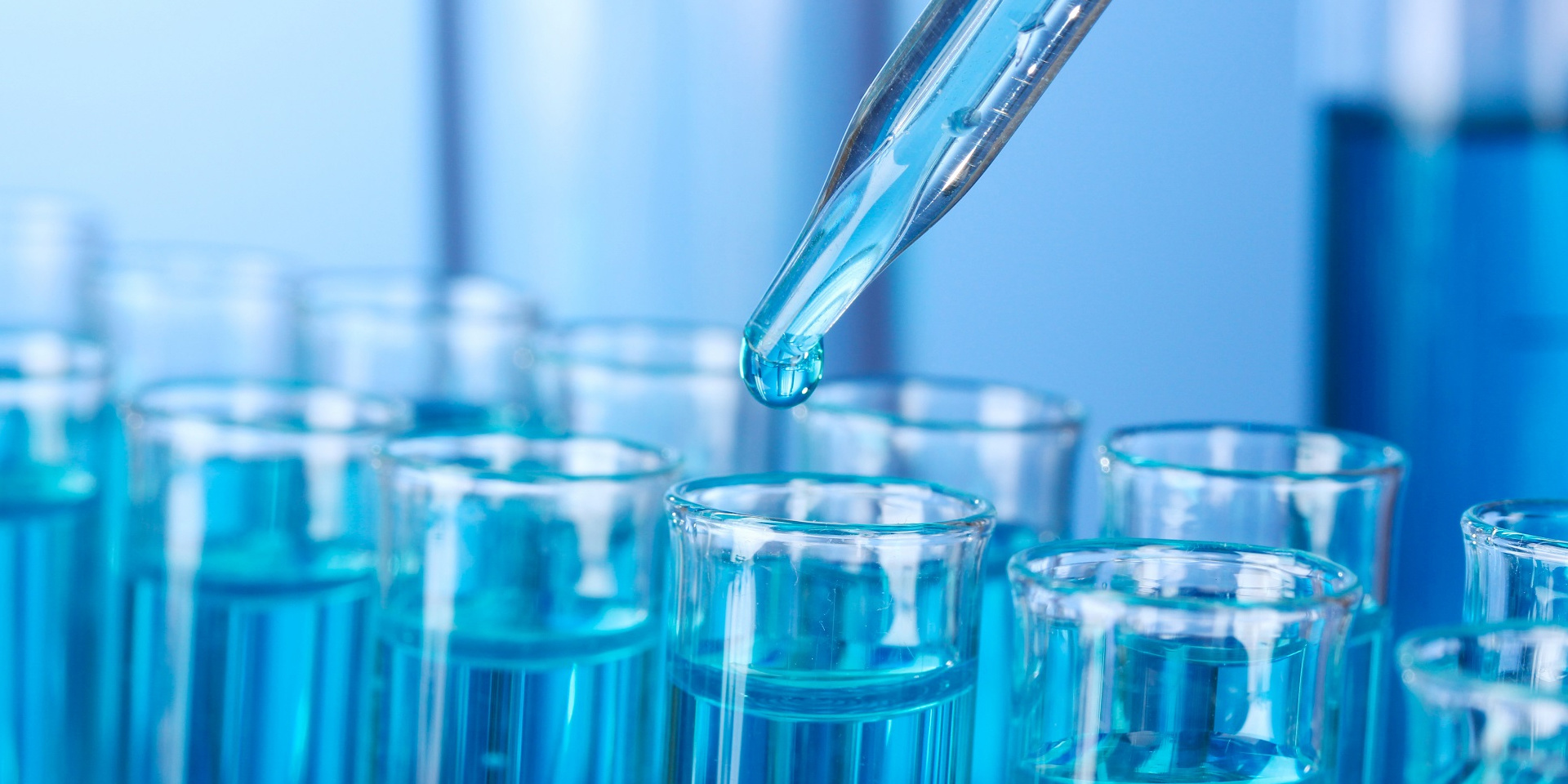
Hydrometallurgy for PCBs is divided into acidic and alkaline methods:
- The acidic method is more precise and cost-effective but time-consuming. This method is suitable for inner layers because acids do not react with photoresists and will not damage the required parts.
- The alkaline method is used for etching the outer layers of PCBs. It is a fast process but more expensive, and it is essential to carefully follow the process parameters because prolonged contact with the solvent can damage the circuit board.
Existing etching solutions typically use hydrogen peroxide or sodium persulfate as the oxidizing agents to remove excess graphite, carbon black, and metal impurities in the processes of wiring printing, micro-etching, and circuit board cleaning. Hydrogen peroxide oxidizes the metals, partially decomposes them, and then converts them into soluble compounds. For instance, products based on sodium persulfate can be combined with sufficient sulfuric acid to create a micro-bath, with 100-300 grams of sodium persulfate per liter of deionized water, containing approximately 1% to 10% by weight of sulfuric acid. However, technicians have recently discovered that Potassium Monopersulfate can serve as an excellent alternative because it contains both the necessary oxidizing agent and sulfuric acid.
*JHY's electronic-grade Potassium Monopersulfate finds application in etching or micro-etching surfaces to reduce thickness, remove oxidation layers, and pre-clean before metal bonding or plating. Our Products have been widely exported to various countries and regions. Please find JHY domain experts for more details.
|
JHY,Your Trusted Partner
We not only have standardized products but also provide a one-on-one customized solution. No matter what challenges we meet, we solve them together. Should you have any questions or needs related to PCB Etching, please do not hesitate to contact our domain experts.
|
 |
Key words: potassium hydrogen peroxymonosulfate compound salt, sodium percarbonate, sodium perborate, calcium peroxide, magnesium peroxide, solid hydrogen peroxide, magnesium silicate, magnesium aluminum silicate, composite powder, oil filter powder, anthraquinone regeneration catalyst
Related Products


24-hour service hotline:
E-mail:
Office Address:
Room 701, Building 2, Rafael Sky City, Lane 288, Qianfan Road, Xinqiao Town, Songjiang District, Shanghai, China
Business License SEO TagsTechnical Support:China Enterprise Power Puxi